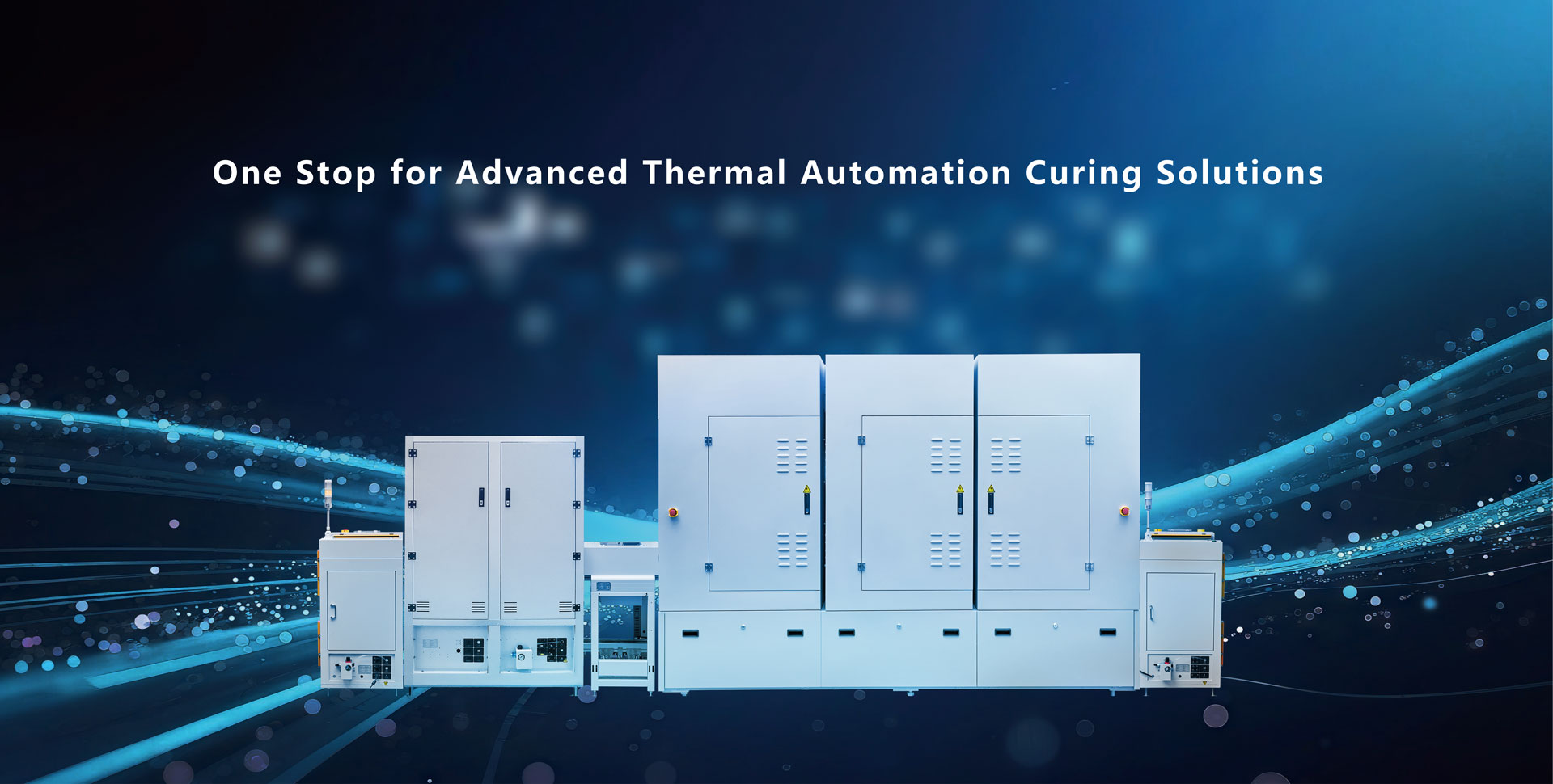
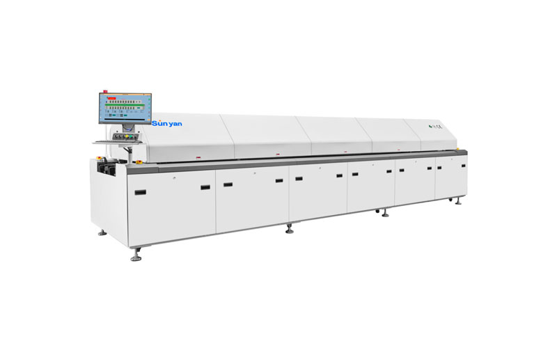
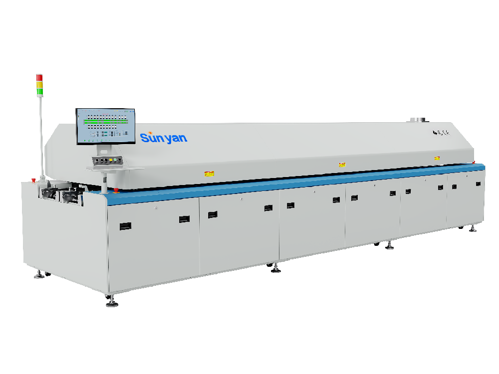
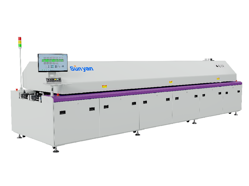
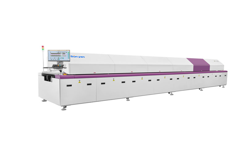
Product Centre


Application
Application
-


Consumer Electronics
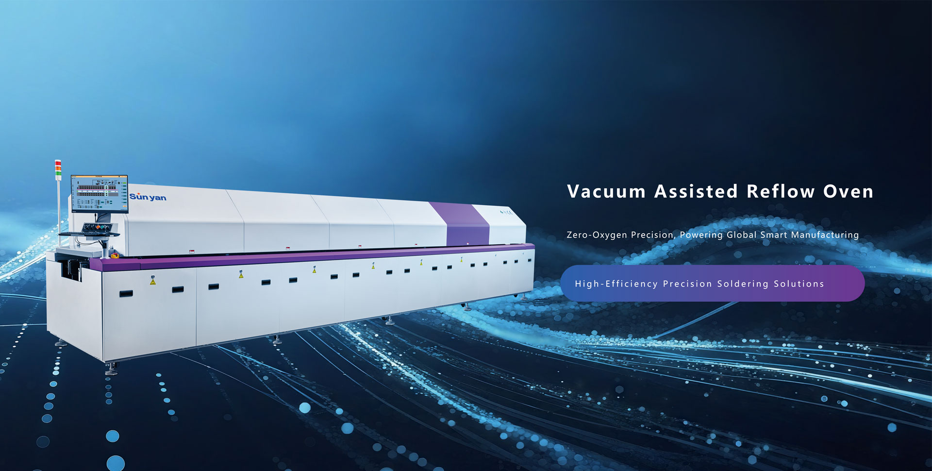
Solution: Provide fully automatic vacuum reflow soldering, in-line vertical curing oven and other equipment. Fully-automatic vacuum reflow soldering can accurately control the soldering temperature and time to ensure the high quality and reliability of electronic component soldering, and avoid the f
-

Aerospace Military Industry
Aerospace Military Industry SolutionsPain point analysis Aerospace military products have extremely high requirements for quality and reliability, and the production process needs to strictly follow the relevant national and industry standards and norms. The production of products involves a v
-

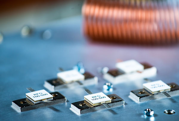
Cell phone communication
Solution: For the soldering and curing process of key components such as cell phone motherboards, we provide equipment such as semiconductor reflow soldering and in-line high-clean oxygen-free vertical curing ovens. Semiconductor reflow soldering can meet the demand for high-precision soldering of t
-

Automotive electronics
Solution: Automotive electronics requires high reliability and stability of equipment, Amazing Grace's IGBT Vertical Curing Oven and Vacuum Pressure Oven can meet the requirements. IGBT Vertical Curing Oven is used for curing automotive electronic power devices to ensure the stable performance o
-

Medical care
Solution: In medical equipment manufacturing, such as welding of electronic components and curing of coatings for medical devices, we provide equipment such as fully automatic vacuum reflow soldering and in-line vertical curing ovens. These equipments can ensure that the welding of electronic compon
-
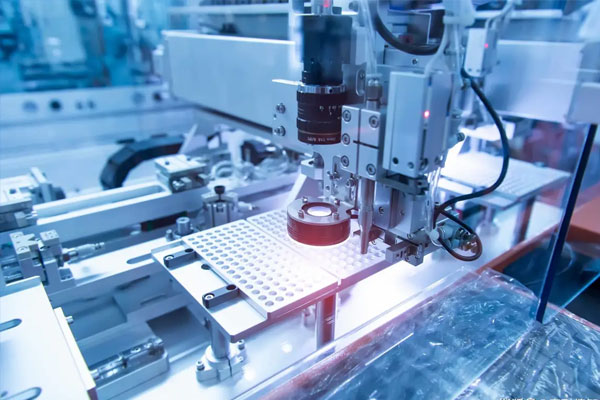
Semiconductor industry
Solution: The production process of semiconductor industry requires high precision and stability of the equipment, Amazing Grace's semiconductor reflow soldering and IGBT vertical curing oven can provide powerful support for it. Semiconductor reflow soldering can realize high-precision soldering
About Us
About Us
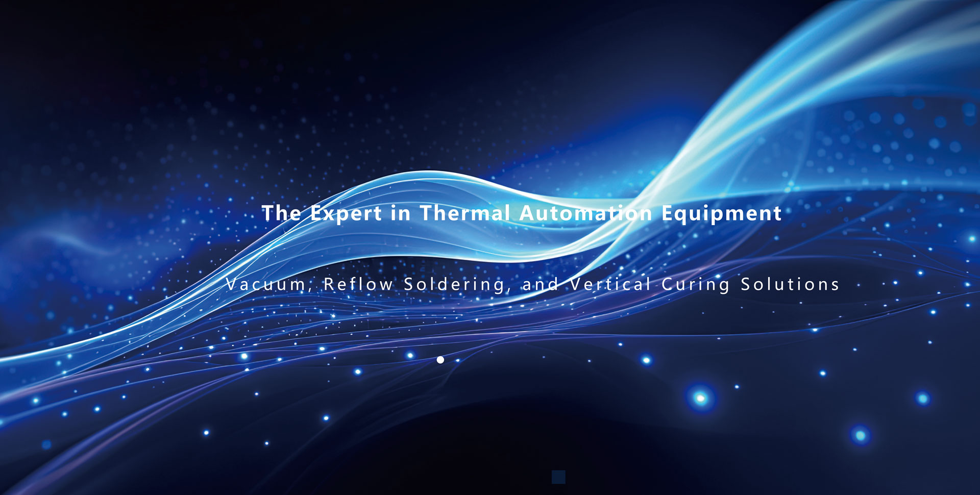
Guangdong Sun yan Thermal Technology Co., Ltd. (referred to as "Sun yan ") is an innovative company specializing in the field of thermal automation equipment. It is an outstanding provider of thermal equipment, integrating research and development, manufacturing, and services.
The company adheres to the business philosophy of "Driven by technological innovation, Guided by customer needs, Based on reliable quality, Aiming at win-win cooperation" striving to enhance production efficiency, reduce costs, and facilitate intelligent transformation and upgrading for customers across various industries through the innovative application of automation technology. We firmly believe that only by continuously pursuing excellence and staying customer-oriented can we stand out in the fierce market competition and become a leader in the thermal automation equipment industry.
Sun yan collaborates with top domestic universities and research institutes for joint technological development, bringing together a team of professionals from the automation field, covering mechanical design, electrical control, software development, and thermal engineering. With keen market insight, outstanding technical expertise, and a dedicated craftsmanship spirit, we are committed to providing customers with efficient, stable, and advanced equipment solutions, driving technological progress and development in the industry.
Our equipment, including vacuum reflow soldering machines, semiconductor reflow soldering machines, inline vertical curing oven, inline high-cleanliness oxygen-free vertical curing oven, IGBT vertical curing oven, vacuum pressure ovens, and more, is widely used in consumer electronics, mobile communications, automotive electronics, medical, aerospace and military, and semiconductor industries. We have helped numerous customers achieve automation and intelligence in their production processes, generating significant economic and social benefits.
-
Industry experience
10+
-
Technical Team
15+
-
Patents for inventions
10+
-
Clients
100+


News
News Center

-

2025-09-16
SMT reflow process core analysis
-
2025-09-16
SMT process lecture hall: how to use the vertical curing oven to solve the PCBA warping and heat-sensitive components damage problems
-
2025-08-14
With the rise of third-generation semiconductor (SiC/GaN) packaging, how does vacuum reflow address its key soldering challenges?

Corporate culture
Company culture
-
Mission
Make soldering and curing more efficient and more reliable.
Provide high-quality equipment for electronics manufacturing, new energy, military, medical, and semiconductor industries, helping customers improve efficiency, optimize processes, reduce energy consumption, and drive the development of smart manufacturing.
-
Vision
To become the top global supplier of thermal solutions for semi-Con and SMT manufacturing
Driving the future of electronic manufacturing with intelligent, sustainable, and highly reliable technologies.
-
Values
Integrity First,Quality First,Continuous Innovation,Customer First,Win-Win Cooperation.
-
Business philosophy
Driven by technological innovation, Guided by customer needs, Based on reliable quality, Aiming at win-win cooperation
Clients
Clients